

")
Important: The printed circuit boards are prepared for different assembly variants, components are not required in all component positions. Assembly variants are marked in the circuit diagram by connections which do not run vertically or horizontally. Familiarize yourself with the schematic diagram (ACSI2SD Mod, ACSI2SD Proc), the bill of materials and the PCB first.
Practical help for soldering SMD components is offered by all kinds of tutorials on the internet, e.g. www.mikrocontroller.net
Should individual components become unusable during assembly, they can be reordered from our webshop (observe the minimum order value!)
ACSI2SD Kit Mod (module version):
-
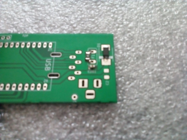
Solder 3 SMT components on TOP side
-
Solder SMT LED and resistor on BOTTOM side.
These 2 parts can be soldered either for "SD active" display (upper position) or "Power" display (lower position).
SD active will be displayed also by the blue LED on CY8CKIT module on the reverse side, so if these components are difficult for you to solder, this step can be omitted.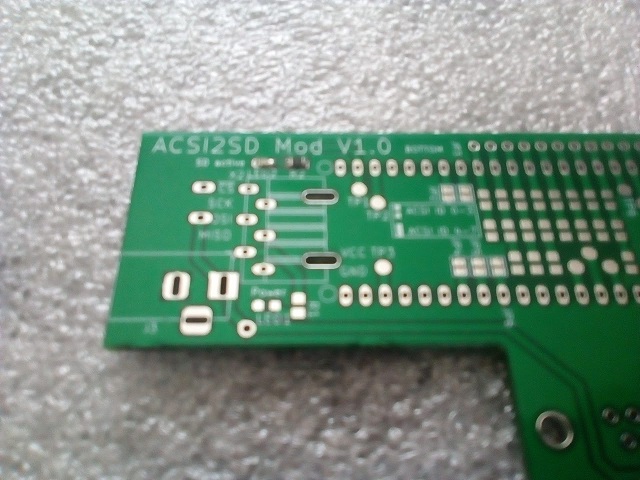
-
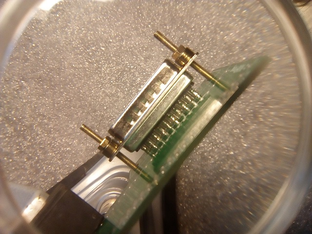
Solder the DSub19 connector. We recommend to lock the connector against the board with 2 screws, then solder short solid pieces of wire, which should be as thick as possible, first into the solder cup of the connector and then on the other side of the circuit board.
-
Program the module CY8CKIT-059, configure it with the program SCSI2SD-util, then disconnect (snap-off) programmer.
This point is omitted in the Easy version, the module of this version is already programmed. It is pre-configured to ACSI ID 1-4. The SCSI ID configuration can be changed at any time with SCSI2SD-util. The ACSI ID to SCSI ID mapping can be changed in the LUT table in PSoC Creator and by solder jumper.
-
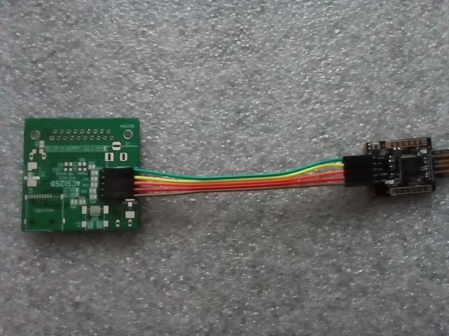
Solder the module CY8CKIT-059 onto the ACSI2SD PCB, there are several solutions:
a. Using 52 about 8mm long pieces of wire: leave about 2-3mm distance between the circuit boards, with around 1.6mm PCB thickness, the wire should protrude then still about 1mm on each side. The distance between the circuit boards should be chosen so that you can disconnect the module using a small side cutter by cutting the wires and possibly use the module elsewhere.
b. with DIL pin headers, not recommended, as long pin headers are difficult to desolder in case you want to reuse the module
c. with sockets like an IC. Then pay attention to their height, because there will be only 10mm distance between the Atari housing and the ACSI2SD PCB. - Prepare the 6-pin microSD card connector: fit into the plated through holes and solder the 6 pins.
If a flat (Arduino type) connector is used: bend 2 x 3 connections each 90°, so that zigzag pattern is created. The black connector body should touch the PCB.
Later, you can attach the MicroSD adapter board firmly by a piece of foam like in the picture below and a piece of wire running across the adapter pressing it down.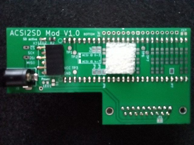
- Solder the DC jack J1 for external power supply. The 3 terminals stand far off from the PCB surface. Do not solder a dome up to the tip, just the lower part close to the PCB. By doing so, the upper part can be bent aside or clipped if there is a space constraint between the PCB and your Atari housing.
Those who don't want to use an external power supply can connect a wire between the closest 5V pad in their ATARI ST, feed it through the housing, and connect it to the PTH drilling adjacent to J1.
(Picture below taken with ACSI2SD Proc version).
Those who are not afraid to modify their Atari could internally connect 5V to pin 11 of the ACSI connector, instead of GND, and only with this modification close the jumper JP1. Closing JP1 without modification will result in a short circuit.
After the described modification standard ACSI devices cannot be used at this port anymore, so this is a solution only for users who know exactly what they are doing.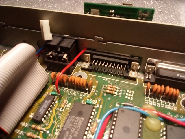
-
Insert your microSD card into the blue card module, insert the card module into the 6-pin connector and test ACSI2SD via USB using the program file SCSI2SD-monitor.
During the test, the assembly is powered by USB from your computer. Consequently we don't need external power nor should the assembly be plugged into ACSI interface of your Atari.
SCSI2SD-monitor will show SCSI "FAIL", please ignore.
SCSI2SD-monitor tests also the microSD interface, thus it needs an inserted microSD card.
We recommend to fix a small piece of foam with double-side tape at the position like in the picture to prevent the card module to rub or scratch against the PCB.
Video of a buyer with his method:
ACSI2SD Kit Proc (QFP100 processor version):
-
Solder U1 (PQFP100), pay attention to the orientation, compare with photos. The alignment with respect to the pads must be very accurate, it is time-consuming to de-solder a PQFP100. Visually and possibly also electrically check for contact between pin and pad, as well as unintended solder bridges between pins.
-
Solder 100nF and 1uF capacitors adjacent to U1. Without this step, programming of U1 may fail.
Steps 3,4,5 can be omitted if your kit contains a pre-programmed microcontroller.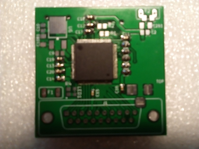


-
Solder 5-pin programming plug X5. First align one pin, then align pins parallel to the PCB, then solder the remaining pins. When programming with MiniProg3, solder the 10-pin SMD connector X4 (not included).
-
Connect 5-pin programming cable with programming plug X5 on one side and KitProg on the other side, pay attention to the same signals at both ends.
-
Plug KitProg into your computer's USB port and program from PSoC Creator, then unplug the programming cable from the programming plug.
When programming, SCSI2SD is powered from your computer via USB and then through KitProg.
-
Solder remaining SMD components, preferably the smaller ones first, then the larger ones (MicroSD, USB connectors). For diodes and ICs, it is important to observe the orientation.
-
Insert MicroSD card into socket, connect USB cable (not included) between your computer and USB connector and configure the whole module with the program SCSI2SD-util and test it with the program SCSI2SD-monitor.
During the test, the assembly is powered by USB from your computer.
SCSI2SD-monitor will show SCSI "FAIL", please ignore.
SCSI2SD-monitor tests also the microSD interface, thus it needs an inserted microSD card.
When configuring and testing, check the function of the LED. There is only one LED and one serial resistor contained in your kit. These both components can either be used to display "Power" or "SD active". We recommend to use for "SD active", those who want to display "Power" in addition can mount a cheap 0603-LED in their desired color and a 0805 serial resistor which need to be bought separately.
-
After successful testing solder the ACSI connector or 19 terminal pins.
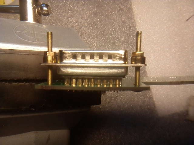
Terminal pims: In order to get all terminals exactly into vertical position, we recommend to clamp a spare female DSub25 (or higher pin count) connector in a vice, insert the terminal pins upside down, cover them with the PCB and solder pin by pin. Take care to use enough flux, so that the solder can flow down the plated hole up to the cuff and by that stabilizes the terminal pin. Tin-plated 10mm terminals should not be fully driven into the PCB. The cuff should be located 1-2mm above the PCB, slightly higher than the highest components on TOP side. By that, the assembly can be pushed into the mating connector up to the cuff.
If soldered correctly, the assembly will almost touch the Atari housing.
DSub19: For DSub19 we recommend to lock the connector against the board with 2 screw connections, then solder short, solid pieces of wire, which should be as thick as possible, first into the solder cup of the connector and then on the other side of the circuit board.
If soldered correctly, there will be a gap of around 10mm between the PCB and your Atari housing.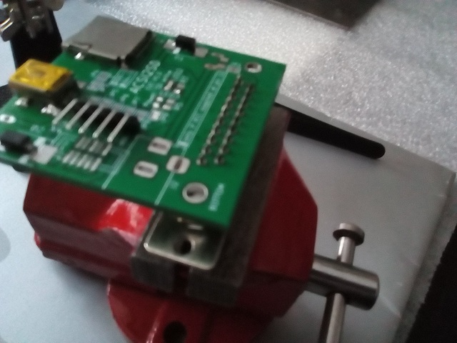
- Solder the DC jack J1 for external power supply. Those who don't want to use an external power supply can connect a short wire between the closest 5V pad in their ATARI ST, feed it through the housing, and connect it to the PTH drilling adjacent to fuse F1.